$
% macros
% MathJax
\newcommand{\bigtimes}{\mathop{\vcenter{\hbox{$\Huge\times\normalsize$}}}} % prefix with \! and postfix with \!\!
% sized grouping symbols
\renewcommand {\aa} [1] {\left\langle {#1} \right\rangle} % <> angle brackets
\newcommand {\bb} [1] {\left[ {#1} \right]} % [] brackets
\newcommand {\cc} [1] {\left\{ {#1} \right\}} % {} curly braces
\newcommand {\mm} [1] {\lVert {#1} \rVert} % || || double norm bars
\newcommand {\nn} [1] {\lvert {#1} \rvert} % || norm bars
\newcommand {\pp} [1] {\left( {#1} \right)} % () parentheses
% unit
\newcommand {\unit} [1] {\bb{\mathrm{#1}}} % measurement unit
% math
\newcommand {\fn} [1] {\mathrm{#1}} % function name
% sets
\newcommand {\setZ} {\mathbb{Z}}
\newcommand {\setQ} {\mathbb{Q}}
\newcommand {\setR} {\mathbb{R}}
\newcommand {\setC} {\mathbb{C}}
% arithmetic
\newcommand {\q} [2] {\frac{#1}{#2}} % quotient, because fuck \frac
% trig
\newcommand {\acos} {\mathrm{acos}} % \mathrm{???}^{-1} is misleading
\newcommand {\asin} {\mathrm{asin}}
\newcommand {\atan} {\mathrm{atan}}
\newcommand {\atantwo} {\mathrm{atan2}} % at angle = atan2(y, x)
\newcommand {\asec} {\mathrm{asec}}
\newcommand {\acsc} {\mathrm{acsc}}
\newcommand {\acot} {\mathrm{acot}}
% complex numbers
\newcommand {\z} [1] {\tilde{#1}}
\newcommand {\conj} [1] {{#1}^\ast}
\renewcommand {\Re} {\mathfrak{Re}} % real part
\renewcommand {\Im} {\mathrm{I}\mathfrak{m}} % imaginary part
\newcommand {\abs} [1] {\nn{#1}}
% quaternions
\newcommand {\quat} [1] {\tilde{\mathbf{#1}}} % quaternion symbol
\newcommand {\uquat} [1] {\check{\mathbf{#1}}} % versor symbol
\newcommand {\gquat} [1] {\tilde{\boldsymbol{#1}}} % greek quaternion symbol
\newcommand {\guquat}[1] {\check{\boldsymbol{#1}}} % greek versor symbol
% vectors
\renewcommand {\vec} [1] {\mathbf{#1}} % vector symbol
\newcommand {\uvec} [1] {\hat{\mathbf{#1}}} % unit vector symbol
\newcommand {\gvec} [1] {\boldsymbol{#1}} % greek vector symbol
\newcommand {\guvec} [1] {\hat{\boldsymbol{#1}}} % greek unit vector symbol
% special math vectors
\renewcommand {\r} {\vec{r}} % r vector [m]
\newcommand {\R} {\vec{R}} % R = r - r' difference vector [m]
\newcommand {\ur} {\uvec{r}} % r unit vector [#]
\newcommand {\uR} {\uvec{R}} % R unit vector [#]
\newcommand {\ux} {\uvec{x}} % x unit vector [#]
\newcommand {\uy} {\uvec{y}} % y unit vector [#]
\newcommand {\uz} {\uvec{z}} % z unit vector [#]
\newcommand {\urho} {\guvec{\rho}} % rho unit vector [#]
\newcommand {\utheta} {\guvec{\theta}} % theta unit vector [#]
\newcommand {\uphi} {\guvec{\phi}} % phi unit vector [#]
\newcommand {\un} {\uvec{n}} % unit normal vector [#]
% vector operations
\newcommand {\inner} [2] {\left\langle {#1} , {#2} \right\rangle} % <,>
\newcommand {\outer} [2] {{#1} \otimes {#2}}
\newcommand {\norm} [1] {\mm{#1}}
\renewcommand {\dot} {\cdot} % dot product
\newcommand {\cross} {\times} % cross product
% matrices
\newcommand {\mat} [1] {\mathbf{#1}} % matrix symbol
\newcommand {\gmat} [1] {\boldsymbol{#1}} % greek matrix symbol
% ordinary derivatives
\newcommand {\od} [2] {\q{d #1}{d #2}} % ordinary derivative
\newcommand {\odn} [3] {\q{d^{#3}{#1}}{d{#2}^{#3}}} % nth order od
\newcommand {\odt} [1] {\q{d{#1}}{dt}} % time od
% partial derivatives
\newcommand {\de} {\partial} % partial symbol
\newcommand {\pd} [2] {\q{\de{#1}}{\de{#2}}} % partial derivative
\newcommand {\pdn} [3] {\q{\de^{#3}{#1}}{\de{#2}^{#3}}} % nth order pd
\newcommand {\pdd} [3] {\q{\de^2{#1}}{\de{#2}\de{#3}}} % 2nd order mixed pd
\newcommand {\pdt} [1] {\q{\de{#1}}{\de{t}}} % time pd
% vector derivatives
\newcommand {\del} {\nabla} % del
\newcommand {\grad} {\del} % gradient
\renewcommand {\div} {\del\dot} % divergence
\newcommand {\curl} {\del\cross} % curl
% differential vectors
\newcommand {\dL} {d\vec{L}} % differential vector length [m]
\newcommand {\dS} {d\vec{S}} % differential vector surface area [m^2]
% special functions
\newcommand {\Hn} [2] {H^{(#1)}_{#2}} % nth order Hankel function
\newcommand {\hn} [2] {H^{(#1)}_{#2}} % nth order spherical Hankel function
% transforms
\newcommand {\FT} {\mathcal{F}} % fourier transform
\newcommand {\IFT} {\FT^{-1}} % inverse fourier transform
% signal processing
\newcommand {\conv} [2] {{#1}\ast{#2}} % convolution
\newcommand {\corr} [2] {{#1}\star{#2}} % correlation
% abstract algebra
\newcommand {\lie} [1] {\mathfrak{#1}} % lie algebra
% other
\renewcommand {\d} {\delta}
% optimization
%\DeclareMathOperator* {\argmin} {arg\,min}
%\DeclareMathOperator* {\argmax} {arg\,max}
\newcommand {\argmin} {\fn{arg\,min}}
\newcommand {\argmax} {\fn{arg\,max}}
% waves
\renewcommand {\l} {\lambda} % wavelength [m]
\renewcommand {\k} {\vec{k}} % wavevector [rad/m]
\newcommand {\uk} {\uvec{k}} % unit wavevector [#]
\newcommand {\w} {\omega} % angular frequency [rad/s]
\renewcommand {\TH} {e^{j \w t}} % engineering time-harmonic function [#]
% classical mechanics
\newcommand {\F} {\vec{F}} % force [N]
\newcommand {\p} {\vec{p}} % momentum [kg m/s]
% \r % position [m], aliased
\renewcommand {\v} {\vec{v}} % velocity vector [m/s]
\renewcommand {\a} {\vec{a}} % acceleration [m/s^2]
\newcommand {\vGamma} {\gvec{\Gamma}} % torque [N m]
\renewcommand {\L} {\vec{L}} % angular momentum [kg m^2 / s]
\newcommand {\mI} {\mat{I}} % moment of inertia tensor [kg m^2/rad]
\newcommand {\vw} {\gvec{\omega}} % angular velocity vector [rad/s]
\newcommand {\valpha} {\gvec{\alpha}} % angular acceleration vector [rad/s^2]
% electromagnetics
% fields
\newcommand {\E} {\vec{E}} % electric field intensity [V/m]
\renewcommand {\H} {\vec{H}} % magnetic field intensity [A/m]
\newcommand {\D} {\vec{D}} % electric flux density [C/m^2]
\newcommand {\B} {\vec{B}} % magnetic flux density [Wb/m^2]
% potentials
\newcommand {\A} {\vec{A}} % vector potential [Wb/m], [C/m]
% \F % electric vector potential [C/m], aliased
% sources
\newcommand {\I} {\vec{I}} % line current density [A] , [V]
\newcommand {\J} {\vec{J}} % surface current density [A/m] , [V/m]
\newcommand {\K} {\vec{K}} % volume current density [A/m^2], [V/m^2]
% \M % magnetic current [V/m^2], aliased, obsolete
% materials
\newcommand {\ep} {\epsilon} % permittivity [F/m]
% \mu % permeability [H/m], aliased
\renewcommand {\P} {\vec{P}} % polarization [C/m^2], [Wb/m^2]
% \p % electric dipole moment [C m], aliased
\newcommand {\M} {\vec{M}} % magnetization [A/m], [V/m]
\newcommand {\m} {\vec{m}} % magnetic dipole moment [A m^2]
% power
\renewcommand {\S} {\vec{S}} % poynting vector [W/m^2]
\newcommand {\Sa} {\aa{\vec{S}}_t} % time averaged poynting vector [W/m^2]
% quantum mechanics
\newcommand {\bra} [1] {\left\langle {#1} \right|} % <|
\newcommand {\ket} [1] {\left| {#1} \right\rangle} % |>
\newcommand {\braket} [2] {\left\langle {#1} \middle| {#2} \right\rangle}
$
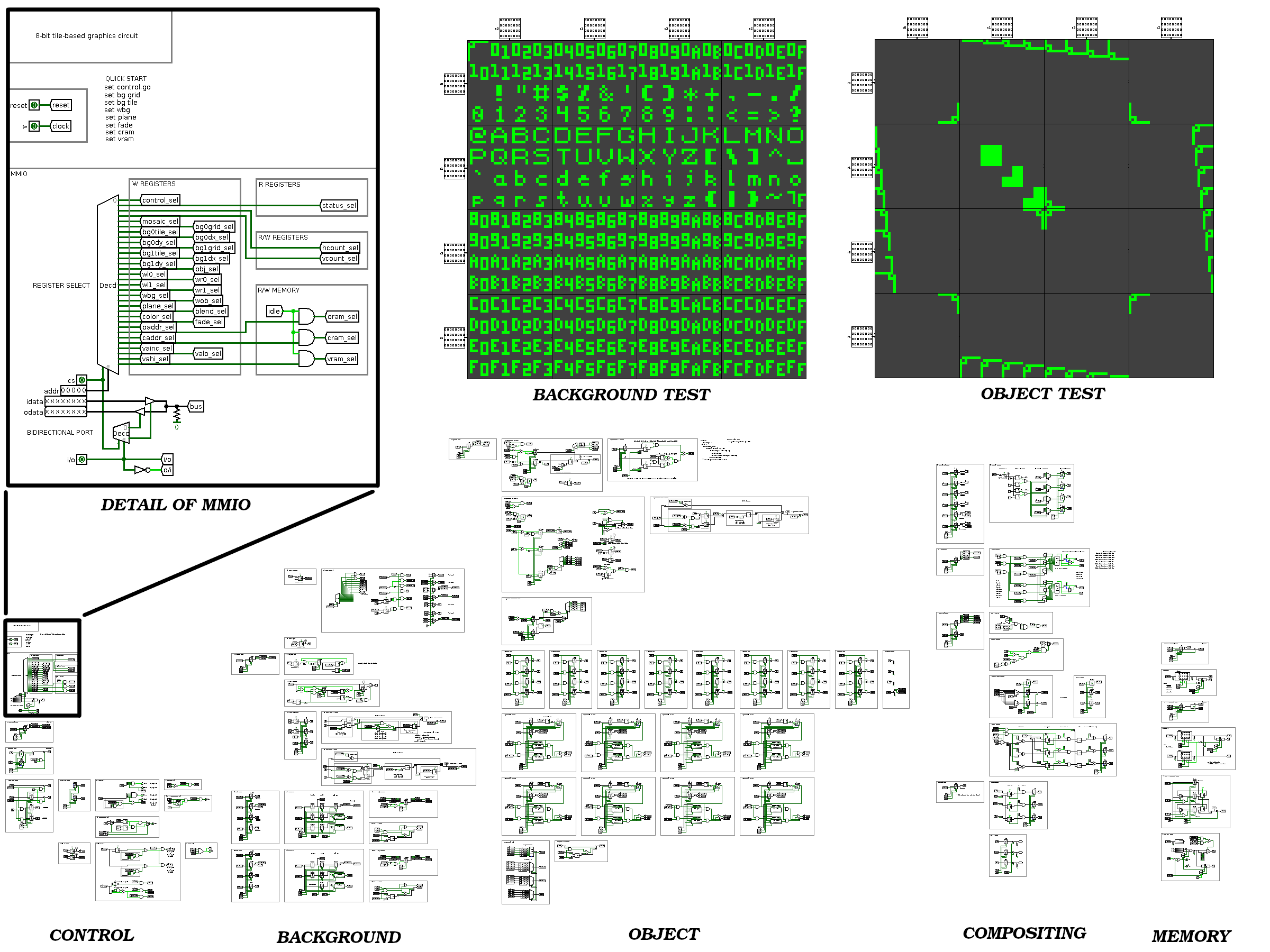
8-bit Tile-Based Graphics Circuit Emulator
In-browser debugging emulator for my tile-based GPU design.
UI Notes
Batches are periodically scheduled to run when the Run checkbox is checked.
Unchecking the checkbox stops the scheduling of batches.
Pressing the Step button while Run is checked also stops the scheduling of batches.
Pressing Step when Run is not checked causes the emulator to run 1 tick.
Emulation run control is concentrated in the debug panel.
The
The Break checkbox enables the breakpoint, and the hbreak and vbreak bytes specify its location.
Keep in mind, the worker processes command messages from the main thread only following a batchpoint or breakpoint.
This is can be confirmed by reading hcount and vcount.
debug
Reset - clear GPU registers and memories
Run - toggle GPU running state
Step - if GPU running, stop GPU, else tick emulation
loop tab - periodically calls a script in the main thread
Save - button - save script to local storage
Load - button - load script from local storage
Enable - checkbox - enable loop
Delay - number4 - loop delay in milliseconds, in range of (0, 9999)[ms]
trace - panel - selectively trace circuit signals and registers in console (F12)
timing - checkbox - trace timing circuit
bg - checkbox - trace background circuit
obj - checkbox - trace object circuit
comp - checkbox - trace compositing circuit
mem - checkbox - trace memory circuit
Implementation Details
The aim is to faithfully reproduce the digital logic of the GPU in software for debugging and evaluation.
It is a massive improvement over the logisim implementation in terms of performance, color display, and sharability.
The program is multi-threaded.
The main thread maintains the debugger interface.
The (web) worker thread emulates the circuit and asynchronously renders to a display canvas.
The threads communicate by builtin message queues.
Each thread has a message queue that any thread can send messages to (Window.postMessage(), Worker.postMessage()).
Each thread also sets a handler function (.onmessage) to receive messages.
A thread's event loop periodically checks the message queue.
Received messages are dequeued and passed to the handler.
For the debugging emulator, the following messaging guideline is used:
In general, the main thread sends command messages and handles UI update messages, and the worker handles command messages and sends UI update messages.
By design, the main thread does not directly update its worker-dependent UI widgets, it indirectly updates them handling UI update messages.
This configuration ensures that the UI accurately represents the worker's state.
The digital logic emulator functions at pixel clock granularity.
A tick amounts to evaluating all combinational logic and then updating all sequential logic.
A pixel is also rendered conditional on display timing and based on color output.
The worker runs emulation ticks in batches.
This allows the worker to periodically yield to its event queue and handle incoming messages.
Yielding is critical to responsiveness, but waiting to be rescheduled takes time, and must be balanced against batch size.
Batch size can be as small as a single tick in a pixel, to as large as 65536 ticks in a display cycle.
A batch size of a pixel yields frequently, resulting in slow emulation, allowing one to view the raster update.
A batch size of a display yields after rendering a full display, and results in the fastest emulation at the cost of responsiveness.
An hv coordinate that coincides with the end of a batch is a batchpoint.
The worker yields at batchpoints, which predict and explain hcount and vcount reads.
Batches are scheduled to run in two different ways.
The first way is by starting the emulator, which causes batches to be periodically scheduled to run.
The second way is by manually stepping the emulator one tick at a time.
A breakpoint can be set to stop the emulator at specific hv coordinates.
If the breakpoint is enabled, when the hv counters equal the breakpoint coordinates, the emulator is stopped and the breakpoint is disabled.
This aids in quickly running the emulator to particular points in the display cycle for inspection and debugging.
The primary way to interact with the GPU is through the MMIO interface.
It consists of a 5-bit address bus, 8-bit data bus, a read/write select, and a chip select.
In practice, the CPU would select the GPU and indicate reading or writing, present a 5-bit address, and read or write from the GPU bus when ticked.
This is too primitive of an interface for a human to use.
Instead the UI provides some conveninces where it can.
Most of the MMIO registers are write-only and are not modified by the GPU in any way;
these have a white input field, and the value is immediately written to the GPU on input.
A single MMIO register is read-only, and clears the contents of the GPU register on read;
this has a gray output field, and a read must be explicitly performed.
The other registers are read/write and have other side effects upon access.
In these cases, a read or write must be explicitly performed.
These controls mimic* how the CPU would interact with the GPU, to the point where the GPU rejects writes if it is busy.
*[The MMIO inputs and outputs replicate the behavior of accessing the graphics circuit by its MMIO port.
This can have side-effects, such as incrementing address registers or clearing the status register.
However, using the MMIO does not tick the pixel clock!!!
Writing this note makes me realize this is a bug not a feature]
The various video memory regions are cumbersome to manipulate by MMIO.
Hex editors have been included to make editing these memories substantially easier.
These editors can be used to save/load local files and copy/paste data.
The hex editors "tweak" the underlying emulator memory with no restrictions and no other side effects.
Implementing this has allowed me to catch and fix a bug in the object circuit. It has also allowed me to see what the output is capable of for the first time.
There's some room for improvement.
The emulator was manually translated from the digital logic. Performance could be improved arranging program by gate depth and possibly adding hints.
A option to defer syncing editor while running emu. Implement a help panel. Add a bit more to the status messages. Shade grid mirror. Improve mouse behavior. Add editor keyboard shortcuts. Put editor drawing code in worker thread and pass drawing commands to it.
8-bit Tile-Based Graphics Circuit
This is the beginning of a series of blog posts detailing the design of a tile-based graphics circuit, pictured below:
My goal for designing this circuit was to work out how tile-based graphics hardware functions.
The design itself is entirely original, but the capabilities are modeled after various 2D video game consoles I grew up playing, namely the SNES.
That was not my original intention!
At the outset I simply wanted to work out the digital logic needed to realize a teletype terminal's display.
However, the resulting circuit wasn't very complicated, which encouraged me to add features.
Things spiraled until I had a design somewhere in capability between an NES and SNES, being closer to the latter.
With a design now in hand, I'd like to realize it in software, FPGA, and hardware.
The journey so far has been very interesting, and I'd like share the story with others.
I have no idea where else you can find this kind of information!
Before continuing, I should mention that the circuit was designed using Logisim.
Tile-Based GPU Specifications
Parameter
Value
Display Resolution
128x128 or 128x112 pixels
Color output
9 bit RGB
Backgrounds
2
Background Grid Size
16x16 units
Background Array Size
1x1, 1x2, 2x1, or 2x2 grids
Background Capabilities
HV scroll, HV flip, 1-bit priority
Objects
64
Object Size
1x1 units
Objects Units Per Scanline
16
Objects Tiles Per Scanline
24
Object Capabilities
HV scroll, HV flip, 2-bit priority
Tile Resolution
8x8 pixels
Tile Colors
2 or 4 colors
Tile Palettes
16
Units
1x1 or 2x2 tiles
Compositing Capabilities
windowing, priority, blending, dithering, fade
Object RAM (ORAM)
256 bytes (internal)
Color RAM (CRAM)
64 bytes (internal)
Video RAM (VRAM)
8192 bytes (external)
When designing a tile-based GPU, the very first thing one must decided upon is what display technology to target.
To the uninitiated, it is not obvious that the display's signal timing largely informs the design of a tile-based GPU.
Old video game consoles targeted CRTs, which aren't widely available anymore.
However, many of the same concepts are applicable to VGA, which some computer monitors still support, either natively or through the DVI port.
Therefore, I decided to target VGA-like displays.
Simulating a full VGA display in Logisim would be computationally expensive, so I decided to implement a caricature of a VGA display.
This caricature retains all of the features of a VGA display, just with non-standard timing.
The display I designed is the most Logisim-oriented component of this work, and takes some explanation.
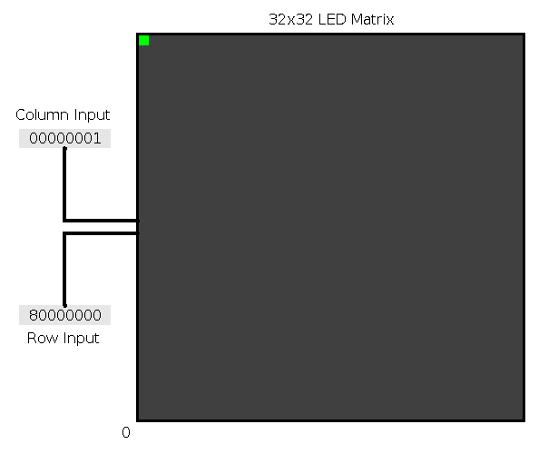
Logisim provides an LED matrix component that can be used to realize a 1-bit display (which is better than nothing!).
An LED matrix can be up to 32x32 pixels.
Each row and column in an LED matrix has a corresponding 1-bit input.
For compactness, Logisim bundles all row and column inputs together into a row and column bus.
In this arrangement, the first bit of the row and column bus corresponds to the bottom row and left column, respectively.
To turn an LED matrix pixel on, the corresponding row and column input must BOTH be driven high at the same time.
This causes the LED to illuminate for a component-specified number of ticks, which allows an image to persist after it's been drawn.
Fig. 1 - Logisim 32x32 LED matrix. Row and column inputs are in hexadecimal.
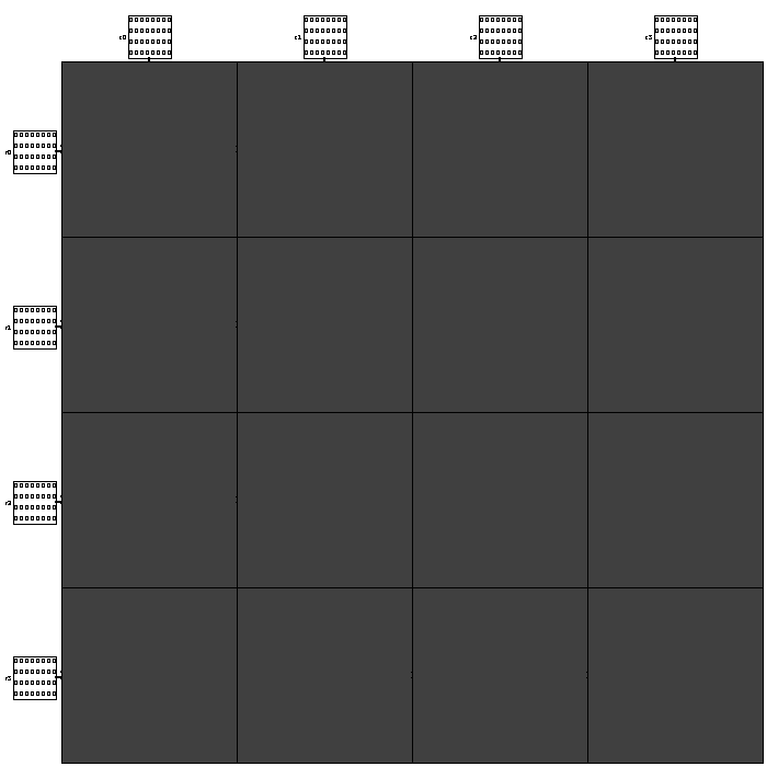
An LED display with arbitrary resolution can be realized by tiling LED matrices.
For this project, I decided to work with 8-bit numbers as much as possible, which can encode up to 256 numbers.
I settled on a 128x128 pixel display (for reasons that will become apparent in a moment), which is composed of 4x4 LED matrices.
I've hidden the bus lines behind the LED matrices, mouse over the image to see them.
Fig. 2 - 128x128 LED display. Row and column inputs are in binary.
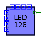
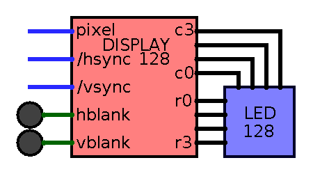
The LED display is conveniently packaged into its own component.
Fig 3. - LED 128 component
With a fat LED matrix in hand, we need a circuit to drive it!
This is where I take inspiration from VGA.
A VGA display is driven by only 5 control lines; 3 analog lines for red, green and blue color information, and 2 digital lines called /hsync and /vsync.
In addition, a VGA display contains an internal pixel clock.
VGA displays draw pixels one at a time, and the pixel clock is incremented exactly once for each pixel drawn.
Image data is streamed to a VGA display as a sequence of pixels organized into a sequence of lines.
Pixels are drawn as they arrive from left to right, and lines are drawn from top to bottom.
This puts the origin of the image in the top left corner of the display.
VGA also includes horizontal and vertical blanking periods when no pixel data is drawn.
These periods are referred to as hblank and vblank.
In CRTs, hblank and vblank gives the electron gun time to reposition itself in preparation to draw the next line or frame, respectively.
The synchronization signals /hsync and /vsync are asserted during their respective blanking periods to synchronize GPU and display operation.
(As an aside, the slashes preceding /hsync and /vsync indicate that they are active when pulled low).
VGA specifies different signal timing for different resolution displays.
There is no 128x128 pixel VGA display, so I invented my own display timing.
Adhering fetishistically to 8-bits, my display timing is framed around 256x256 pixels.
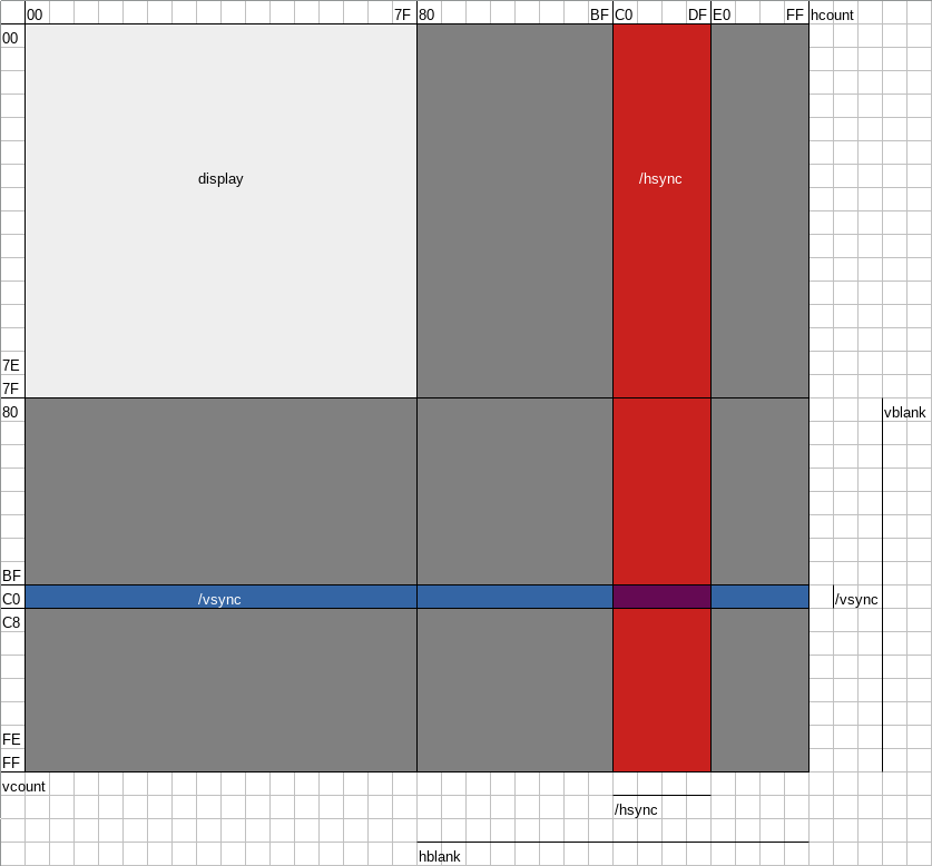
In my design, the horizontal position is labeled hcount and the vertical position vcount.
Hblank occurs during hcount [0x80, 0xFF] and /hsync is expected to be asserted during hcount [0xC0, 0xDF].
Likewise, vblank occurs during vcount [0x80, 0xFF] and /vsync is expected to be asserted during vcount [0xC0, 0xC7].
Perhaps unexpectedly, the display only spends 1/4 of its time drawing anything.
Fig 4. - Display timing
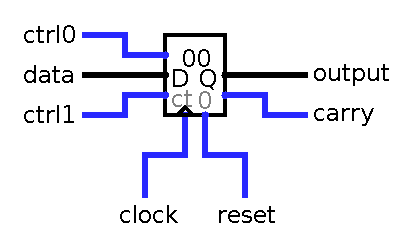
Before looking at the implementation of the display circuit, a brief description of Logisim counters is needed.
Counters are registers with the added ability to be incremented or decremented when clocked.
Two control lines control the function of a counter:
Fig 5. - Counter
Counter Function
ctrl0
ctrl1
Function
0
0
disabled
1
0
load data
0
1
increment
1
1
decrement
The GPU only uses incrementing counters.
When a counter overflows it rolls over to 0 and outputs a carry.
This allows for multiple counters to be chained together.
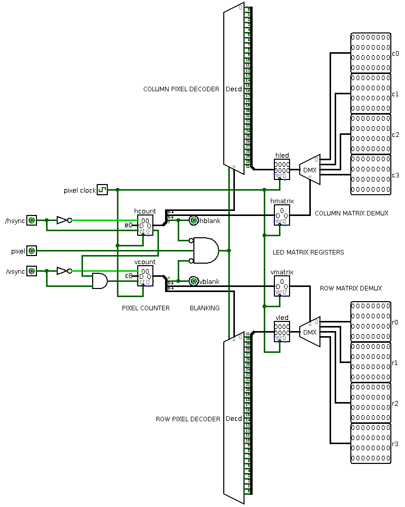
Continuing on, the heart of the display circuit is an internal pixel clock driving a pair of 8-bit pixel counters uncreatively named hcount and vcount.
The counters track what pixel incoming pixel data will be drawn to on the next tick.
The pixel clock increments hcount every tick, while vcount only increments when hcount overflows and outputs a carry (that is, at the end of a line).
When vcount overflows the display cycle starts anew.
In this way all 65536 pixels of the timing diagram are visited in order.
As mentioned before, the pixel clock is independent of the master clock used to run the GPU.
Operation between the GPU and display is synchronized by the /hsync and /vsync control lines, mimicking VGA operation.
When /hsync and /vsync are asserted, the counters are loaded with counts corresponding to the position after their respective synchronization periods.
Upon releasing the syncs, the counters are loaded with a known count, and thus an external circuit (i.e. the GPU) can operate in lockstep with the display.
An AND gate has been added before vcount to ensure incrementing doesn't cause an erroneous decrement during loading by /vsync (see the counter function table).
Pixel data is only accepted by the display when it is not blanking.
In general, detecting the blanking periods requires testing the counters against prescribed ranges using comparators.
However, by judicious choice of timing, detecting the blanking periods in this design is as easy as examining the high bit of the counters.
In this way pixel data is gated by the 3-way AND in the middle of the circuit.
Leveraging powers of 2 like this is a common theme in my design to simplify implementation.
The output of the circuit is particular to the operation of the Logisim LED matrix.
Bits 0-4 of the counters are used to select which of the 32 pixels in a constituent LED matrix row or column is being addressed.
These bits are fed into two decoders to implement a one-hot encoding of the pixel being addressed within a single LED matrix.
A minor detail is that I've reversed the ordering of the rows so that the first bit corresponds to the top row of an LED matrix.
Bits 5-6 of the counters are used to select which of the 4 LED matrices in a row or column is being addressed.
These bits are fed into two demultiplexers that route the one-hot encodings to the correct LED matrix.
With the correct pixel addressed, the actual output is modulated by using the gated pixel data to enable/disable the one-hot encoders.
To prevent transient behavior from incorrectly illuminating pixels, registers have been placed before the demultiplexers to latch output data.
Fig 6. - Display driver circuit
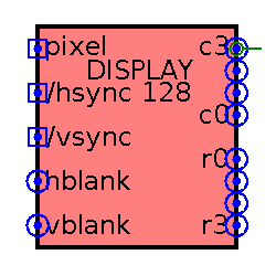
Like the LED matrix, the display circuit is packaged into its own component.
The hblank and vblank outputs have been added for visual debugging, and serve no functional purpose.
Fig 7. - Display driver component
Putting the LED matrix and display circuit together completes the display.
A final detail is that the persistence time for the LED matrices has been set to just under the number of ticks needed to render a full frame.
This allows a drawn image to persist until the next image is just about to overwrite it, similar to how CRT phosphors glow for some time after being stimulated.
Fig 8. - Completed display
While the display circuit is completely independent of the GPU, its timing provides the scaffolding upon which the GPU design turns.
I'll begin describing the basic function of the GPU in the next post.